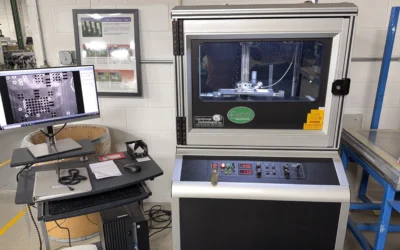
3D AOI PCB inspection, short for 3D Automated Optical Inspection, measures the position, height, shape, and alignment of components and visible solder joints on a printed circuit board assembly.
Unlike traditional 2D inspection, 3D AOI does not rely only on a flat image of the board. It creates a three-dimensional representation of the assembly, allowing it to identify lifted leads, component coplanarity problems, insufficient solder, bridging, polarity errors, placement defects, and other manufacturing issues that may be difficult to detect visually.
Excel Electronics has added a Mirtec MV-6e OMNI 3D AOI system to our SMT production line. It is now integrated into our surface-mount assembly process, providing another layer of automated inspection for the circuit boards we manufacture.
For OEM customers, this means more precise inspection, better process control, and a lower risk of defective assemblies reaching the field.
What Is 3D Automated Optical Inspection?
3D Automated Optical Inspection is a non-contact inspection process that evaluates components, solder joints, and assembly conditions on a printed circuit board.
The system uses high-resolution cameras, controlled lighting, and three-dimensional measurement technology to compare the assembled board against established inspection criteria.
3D AOI can evaluate:
- Component presence
- Component placement
- Component orientation
- Polarity
- Component height
- Lead coplanarity
- Lifted leads
- Lifted components
- Visible solder joint shape
- Insufficient or excessive solder
- Solder bridging
- Tombstoning
- Skewed or rotated components
Because inspection is automated and repeatable, 3D AOI can evaluate production assemblies more consistently than visual inspection alone.
How Is 3D AOI Different from 2D AOI?
The primary difference between 2D and 3D AOI is that 3D AOI measures height and surface geometry.
A traditional 2D AOI system captures flat images of a circuit board. It can identify many common defects, including missing components, incorrect polarity, misalignment, and some visible solder problems.
However, a flat image may not clearly show whether a lead sits directly on the pad or slightly above it. Lighting, shadows, component color, and board reflectivity can also make certain defects difficult to interpret.
A 3D AOI system measures the physical shape and height of components and visible solder joints. This additional data helps distinguish between an acceptable connection and one that is lifted, irregular, tilted, or incorrectly formed.
Why Is Height Measurement Important in PCB Inspection?
Height measurement helps identify defects that may appear acceptable in a top-down image.
For example, a component lead may look aligned with its pad when viewed from above but still be lifted enough to prevent a reliable electrical connection. A component may also be tilted, partially seated, or affected by uneven solder deposition.
By measuring the Z-axis, or vertical dimension, 3D AOI can detect:
- Lifted component leads
- Lifted chip components
- Component tilt
- Coplanarity problems
- Tombstoning
- Uneven component seating
- Irregular solder fillets
- Variations in solder volume
These conditions can cause open circuits, intermittent performance, mechanical weakness, or premature field failure.
What 3D AOI System Does Excel Electronics Use?
Excel Electronics uses the Mirtec MV-6e OMNI, an inline 3D AOI system designed for high-accuracy surface-mount inspection.
The system combines high-resolution imaging, multi-angle inspection, three-dimensional measurement, and automated analysis to evaluate PCB assemblies during production.
What Are the Capabilities of the Mirtec MV-6e OMNI?
High-Resolution Top-Down Imaging
The Mirtec MV-6e OMNI uses a high-resolution CoaXPress vision system to inspect component placement, orientation, polarity, markings, and visible solder conditions.
High-resolution imaging is especially valuable for dense boards, fine-pitch components, and assemblies with small surface-mount devices.
Multi-Angle Side-View Inspection
The system can use multiple side-view cameras to examine components and solder fillets from different angles.
Side-view inspection improves visibility around packages such as:
- J-lead devices
- Gull-wing components
- QFNs with visible side terminations
- Connectors
- Fine-pitch integrated circuits
This helps the system evaluate features that may be obscured or difficult to interpret from a top-down view alone.
Three-Dimensional Height Measurement
The Mirtec system uses Digital Multi-Frequency Quad Moiré technology to measure component and solder joint height.
This enables detection of defects such as:
- Lifted leads
- Lifted components
- Component tilt
- Coplanarity problems
- Tombstoning
- Irregular solder geometry
Inspection of Small Components
The system supports inspection of very small surface-mount components, including 0201 and 01005 package sizes.
These micro-components require precise placement and process control because even minor variations can affect manufacturability and reliability.
What PCB Defects Can 3D AOI Detect?
The specific defects identified depend on the board design, component type, inspection program, and visibility of solder connections.
Common detectable conditions include:
Missing Components
The system can identify components that were not placed or that shifted off the board during assembly.
Incorrect Components
Component markings, dimensions, and programmed characteristics can help identify incorrect parts.
Placement and Alignment Errors
3D AOI can detect components that are offset, rotated, skewed, or improperly aligned with their pads.
Polarity Errors
The system can verify the orientation of polarized components such as diodes, capacitors, and integrated circuits.
Lifted Leads
Height measurement can detect leads that appear aligned from above but are not properly seated on the solder pad.
Lifted or Tilted Components
The system can identify components that are raised, angled, or unevenly seated.
Insufficient or Excessive Solder
Visible solder joints can be evaluated for irregular shape, volume, coverage, and fillet formation.
Solder Bridging
The system can identify visible solder connections between adjacent pads or leads that may create an electrical short.
Tombstoning
Tombstoning occurs when one end of a small chip component lifts away from the board during reflow.
Coplanarity Defects
3D measurement can determine whether component leads or terminations are sitting at inconsistent heights.
Can 3D AOI Inspect BGAs?
3D AOI can verify the presence, placement, orientation, alignment, and exterior condition of a Ball Grid Array package.
However, it cannot directly inspect the solder balls hidden underneath a fully assembled BGA.
Defects such as internal BGA voiding, head-in-pillow conditions, hidden bridging, and incomplete ball collapse generally require PCB X-ray inspection.
For boards containing BGAs and other area-array packages, 3D AOI and X-ray inspection serve complementary purposes:
- 3D AOI verifies component placement, alignment, height, and visible assembly conditions.
- X-ray inspection evaluates hidden solder joints beneath the package.
Excel Electronics uses both technologies as part of a layered PCB quality process.
Can 3D AOI Inspect QFN Components?
3D AOI can inspect QFN placement, orientation, package height, coplanarity, and visible side terminations when those features are accessible.
However, the large center thermal pad and much of the solder connection underneath a QFN are hidden from optical inspection.
X-ray inspection may be used when the application requires evaluation of:
- Thermal-pad solder coverage
- Internal solder voiding
- Hidden bridging
- Solder distribution beneath the package
The appropriate inspection method depends on the component design, reliability requirements, and acceptance criteria for the assembly.
Does 3D AOI Detect Solder Voids?
3D AOI may identify surface irregularities in visible solder joints, but it cannot reliably detect internal solder voids hidden inside or underneath a connection.
X-ray inspection is the appropriate method for evaluating internal voiding beneath BGAs, QFNs, thermal pads, and other hidden solder joints.
This distinction is important because 3D AOI and X-ray inspection detect different classes of defects.
Does 3D AOI Replace Functional Testing?
No. 3D AOI does not replace electrical or functional testing.
AOI evaluates the physical board assembly. It confirms whether components and visible solder connections meet programmed inspection criteria.
Functional testing evaluates whether the completed circuit board operates according to the customer’s design requirements.
A board can be physically assembled correctly but still fail because of:
- A defective component
- A firmware issue
- A design problem
- An incorrect component value
- An internal electrical fault
- A connection that cannot be evaluated optically
For this reason, Excel Electronics uses multiple inspection and testing methods rather than relying on a single technology.
How Does Excel Electronics Inspect PCB Assemblies?
Excel Electronics uses a layered quality process designed to identify different types of manufacturing defects.
1. Solder Paste and Process Control
Production controls help verify that solder paste deposition, placement, and reflow conditions are appropriate for the assembly.
2. 3D Automated Optical Inspection
The Mirtec MV-6e OMNI evaluates component placement, height, alignment, polarity
, visible solder joints, and other physical assembly conditions.
3. X-Ray Inspection
X-ray inspection evaluates hidden solder joints and internal structures that cannot be seen optically, including conne
ctions beneath BGAs and QFNs.
4. Functional Testing
Custom full-function test fixtures can verify that completed assemblies perform according to the customer’s specifications.
Each layer addresses a different category of risk.
Why Is Layered PCB Inspection Important?
No single inspection method can identify every possible circuit board defect.
A board may pass optical inspection but contain a hidden BGA solder problem. It may be physically assembled correctly but fail functional testing. It may also pass initial electrical testing while containing a process variation that could affect long-term reliability.
A layered inspection process combines physical, internal, and functional evaluation to provide greater confidence in the finished assembly.
For OEMs, this can help:
- Reduce escaped defects
- Improve manufacturing consistency
- Reduce field returns
- Support root-cause analysis
- Improve traceability
- Protect customer relationships
- Reduce warranty and service costs
When Should an OEM Ask About 3D AOI?
OEMs should discuss 3D AOI when a PCB assembly includes:
- Fine-pitch components
- 0201 or 01005 components
- High component density
- J-lead or gull-wing packages
- Leadless components
- Tight coplanarity requirements
- High-reliability applications
- Complex mixed-technology assemblies
- New product introductions
- Designs with a history of placement or solder defects
It is also important to ask how the manufacturer combines AOI with X-ray inspection and functional testing.
What Should You Ask a PCB Contract Manufacturer About AOI?
When evaluating an electronics contract manufacturer, ask:
- Is AOI performed in-house?
- Is the system 2D or 3D?
- Is AOI integrated into the production line?
- What component sizes can the system inspect?
- Does the system use side-view cameras?
- Can it measure component and lead height?
- How are false calls reviewed?
- How are inspection programs validated?
- Are inspection results documented?
- How is AOI combined with X-ray and functional testing?
- What happens when a recurring defect is identified?
The equipment itself matters, but so do the programming, inspection criteria, operator training, and corrective-action process behind it.
3D AOI at Excel Electronics
Excel Electronics is an ISO 9001:2015-certified electronics contract manufacturer located in Elkhart, Indiana.
We provide PCB assembly, inspection, testing, prototyping, and production support for OEMs in industries including:
- Specialty vehicles
- Industrial controls
- Medical devices
- Office furniture electronics
- Powersports
- LED lighting
- Commercial equipment
Our quality and testing capabilities include:
- Mirtec MV-6e OMNI 3D AOI
- Multiple automated optical inspection systems
- High-resolution X-ray inspection
- Custom functional test fixtures
- IPC-A-610 workmanship standards
- Process validation
- Failure analysis
- Production quality documentation
Our team brings more than 300 years of combined PCB manufacturing experience to customer projects.
Talk to Excel Electronics About Your Next PCB Build
If you are evaluating a PCB contract manufacturer, launching a new design, or looking for greater process visibility from your current supplier, Excel Electronics can review your assembly requirements.
Submit a QUOTE REQUEST or call 574-206-2627.
Our team can discuss your board design, component technologies, production volumes, testing requirements, and whether our capabilities fit your application.
What is 3D Automated Optical Inspection?
3D Automated Optical Inspection, or 3D AOI, is a non-contact inspection process that measures the position, height, shape, alignment, and visible solder conditions of components on a printed circuit board assembly.
How is 3D AOI different from 2D AOI?
Traditional 2D AOI analyzes flat images of a circuit board. 3D AOI also measures height and surface geometry, allowing it to identify lifted leads, tilted components, coplanarity problems, uneven seating, and irregular visible solder joints that may be difficult to detect in a top-down image.
What PCB defects can 3D AOI detect?
3D AOI can detect missing or incorrect components, placement errors, polarity errors, lifted leads, lifted or tilted components, visible solder bridging, insufficient or excessive visible solder, tombstoning, rotation, skew, and coplanarity defects.
Why is height measurement important in PCB inspection?
Height measurement helps reveal defects that may look acceptable from above. A component lead may appear aligned with its pad but still be lifted, tilted, or improperly seated. Measuring the vertical dimension helps identify these conditions before the assembly moves downstream.
Can 3D AOI inspect BGA solder joints?
3D AOI can inspect BGA placement, orientation, alignment, package height, and visible exterior conditions. It cannot directly inspect the solder balls hidden beneath a fully assembled BGA. Hidden BGA defects generally require X-ray inspection.
Can 3D AOI inspect QFN components?
3D AOI can inspect QFN placement, orientation, height, coplanarity, and visible side terminations. It cannot fully evaluate the hidden center thermal pad or all solder connections beneath the package. X-ray inspection may be required for those features.
Does 3D AOI detect solder voids?
3D AOI may identify surface irregularities in visible solder joints, but it cannot reliably detect internal solder voids hidden inside or beneath a connection. X-ray inspection is the appropriate method for evaluating hidden voiding.
Does 3D AOI replace functional testing?
No. 3D AOI evaluates physical assembly conditions such as placement, height, alignment, polarity, and visible solder joints. Functional testing verifies that the completed circuit board operates according to its design requirements.
Why does inline 3D AOI matter?
Inline 3D AOI allows manufacturing defects to be identified close to the point where they occur. Earlier detection can reduce rework, prevent defects from moving downstream, improve process consistency, protect delivery schedules, and reduce the risk of field failures.
What 3D AOI system does Excel Electronics use?
Excel Electronics uses the Mirtec MV-6e OMNI, an inline 3D Automated Optical Inspection system designed for high-accuracy surface-mount inspection, multi-angle imaging, component height measurement, and automated defect analysis.
Is 3D AOI included in Excel Electronics SMT production?
The Mirtec MV-6e OMNI is integrated into Excel Electronics' SMT production process. Applicable surface-mount assemblies are inspected as part of the normal manufacturing workflow, based on the board design, component technologies, production process, and customer requirements.
How does Excel Electronics inspect PCB assemblies?
Excel Electronics uses a layered quality process that can include process controls, 3D automated optical inspection, X-ray inspection for hidden solder connections, and custom functional testing to verify completed board performance.